Exploring Organic Photovoltaics: The Role of Fullerenes and Oligomers in Solar Cells
Organic Solar Cells and OLEDs
In the fascinating field of renewable energy, organic photovoltaics are emerging as a promising solution to meet the growing demand for clean energy. One of the most notable advances in this area is the use of advanced materials such as fullerenes and oligomers, which play a crucial role in the efficiency and stability of these devices.
What are OLEDs and organic solar cells?
Before we delve into the significance of these materials, let’s grasp the essence of OLEDs (Organic Light-Emitting Diodes) and organic solar cells. Although they operate on similar principles, their purposes are quite distinct:
- OLEDs: These devices emit light when an electric current flows through organic materials. They find applications in displays and lighting fixtures.
- Organic solar cells: These cells harness sunlight to produce electricity, using organic materials to capture light energy and convert it into an electric current.
Fullerenes and Their Derivatives: Cornerstones in Organic Photovoltaics
Fullerenes, such as C60 and its derivatives (PC61BM, PC71BM), have been widely employed as electron acceptors in organic photovoltaics due to their outstanding electronic mobility properties and isotropic charge transport. These characteristics enable:
- Efficient electron collection.
- Enhancement of energy conversion efficiency (PCE).
However, they present limitations such as:
- Difficulty in adjusting their absorption range and energy levels.
- Tendency towards thermal aggregation.
- High production costs.
Oligomers as Electron Donor Layers
Oligomers, particularly those based on carbazole and benzodithiophene (BDT) structures, stand out as excellent electron donors. These materials can be designed to have energy levels and absorption ranges complementary to electron acceptors such as fullerenes. Studies have shown that:
- Fluorination of these materials enhances photovoltaic performance by adjusting energy levels and improving morphological stability.
- Combination with non-fullerene acceptors (NFA) can enhance the efficiency of organic solar cells, especially in tandem configurations.
Importance of Interfacial Engineering
A crucial aspect in organic photovoltaic design is interfacial engineering, involving optimization of intermediate layers to enhance charge collection and transport. For example:
- The use of cross-linkable fullerenes (C-PCBSD) as cathodic intermediate layers improves PCE and stability of organic solar cells.
- These materials facilitate electron transport and protect active layers from degradation caused by external factors such as moisture.
Porphyrin-Fullerene Diodes and Their Applications
Porphyrin-fullerene diodes have been extensively studied due to their ability to generate photocurrent through light-induced or electrically induced charge separation. Notable examples include:
- Development of an artificial photosynthetic reaction center using conformationally restricted macrocyclic diporphins attached to fullerenes.
- Generation of photocurrent in thin films of nanocrystalline SnO2 semiconductor from the state of light-induced charge separation in a porphyrin-C60 diode.
Organic Memories: Innovations and Challenges
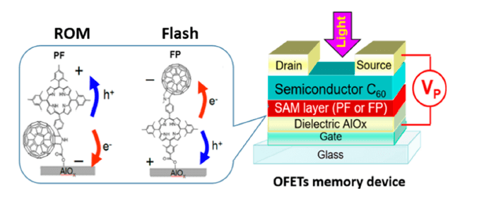
Organic memories represent one of the most dynamic areas of research in organic materials. These devices, including structures such as organic field-effect transistors (OFETs) and resistive memories, offer advantages in terms of flexibility and storage capacity.
Recent Research and Advanced Applications
In a recent study, Nikolaou et al. explored the effect of the triazole ring in zinc-porphyrin-fullerene diodes on charge transfer processes in fully functional devices. These donor/acceptor dyads, based on fullerene as the acceptor material, have led to OFETs and nanostructures in portable electronic devices. Key to flexible, portable, and ultra-light electronics, these devices leverage the high charge mobility in organic materials for applications in sensors, displays, and flexible integrated circuits.
Self-Assembly and Conductivity
Some of these organic structures can self-assemble into linear “pea pod” configurations, exhibiting high electrical conductivity and stability, making them ideal for advanced electronic applications. The ability to efficiently transfer charges over long distances within these materials highlights their potential to revolutionize electronics.
A Promising Future
Advancements in organic memories and the implementation of oligomers and fullerenes in these devices promise to transform current technology, providing more efficient and sustainable solutions for future electronics.
New World Record in Organic Photovoltaics Module Efficiency!
In 2024, the race to optimize the efficiency of organic photovoltaic (OPV) modules reached a significant milestone with a new world record efficiency of 14.5% for the total module area (15.0% for the active area). This breakthrough was achieved by a team of researchers using:
- Computational Fluid Dynamics (CFD) simulations
- Finite Element Method (FEM)
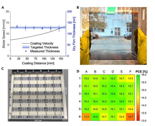
The PM6:Y6-C12 active blend was evaluated over a distance of 165 mm. The goal was to maintain a consistent thickness of the active layer. Thickness measurements at 36 different points (6×6) on a 165 x 165 mm glass/ITO substrate showed remarkable consistency in the coating thickness, which is crucial for ensuring uniform efficiency in individual organic solar cells. The transparency of these photovoltaic systems can also be observed.
Advantages of Organic Photovoltaics
Organic photovoltaics (OPVs) offer unique advantages such as being lightweight, flexible, and transparent, as well as having a low-cost, low-energy production process. Although small cells have reached efficiencies close to 20%, transferring these high efficiencies to larger modules has been a key challenge for effective commercialization.
This new breakthrough marks a significant step towards closing the gap between cell and module efficiencies.
Key Innovations
The research team used Computational Fluid Dynamics (CFD) simulations and the Finite Element Method (FEM) to optimize the uniformity of the coating and the module design.
These simulations led to the development of a blade coating process that achieved a thickness deviation of less than 5% over an area of 200 cm². The PM6:Y6-C12 active material, known for its high efficiency and processability from non-halogenated solvents, was essential to this process.
The uniform coating and module design were optimized to minimize resistance losses and inactive areas. The team achieved a 204 cm² OPV module with a certified efficiency of 14.5%, setting a new world record. This achievement underscores the importance of uniform functional layer coatings and optimized module design to maximize performance.
Fullerenes in Transient Electronics: Towards More Sustainable Electronics
Transient electronics is gaining momentum, offering an environmentally friendly alternative for end-of-life electronic products. These devices are designed to dissolve and disintegrate after a predetermined period. Fullerenes, especially C60, can:
- Control the degradation of transient electronics in printed circuits.
- Trigger the degradation of electronic devices under ultraviolet (UV) light and in the presence of water when combined with polymers like polystyrene (PS).
Studies on Transient Electronics
A team of scientists discovered that adding fullerenes, specifically the fullerene derivative C60-(PCBM), to common non-biodegradable polymers like polystyrene (PS) can trigger the degradation of electronic devices under UV light and in the presence of water.
This means we can control when and how these devices break down, which is crucial for applications like temporary biomedical electronic implants.
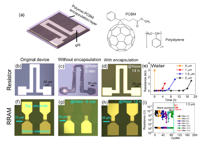
The study shows transient devices encapsulated with a layer containing polystyrene (PS) and PCBM. In the optical images, you can see how a magnesium resistor degrades without encapsulation after immersion in water, whereas with a 2 μm PS layer, the resistor remains intact even after 14 hours of immersion. The resistance of the Mg resistor encapsulated with PS varies with different layer thicknesses.
Additionally, the study demonstrates how a resistive random-access memory (RRAM) remains intact with a PS layer after immersion in water, while it degrades quickly without encapsulation. Finally, the lifespan of a transient RRAM device with a PS layer is investigated through electrical characterization.
The Interaction of Fullerenes with Polymers
The key lies in how fullerenes interact with the polymer. PCBM acts as a photosensitizer, making the polymers more sensitive to UV light, which accelerates their decomposition. This opens the door to a new way of creating electronic devices that can safely disappear when they are no longer needed.


Impact on Organic Electronics and Beyond
This discovery not only benefits organic electronics but can also have a positive impact on electronics in general. Imagine a future where our electronic devices can safely self-destruct when they are no longer needed or become obsolete, leaving no harmful waste behind!
Fullerenes are driving organic electronics towards a brighter and more sustainable future. With their help, we are one step closer to creating electronic devices that not only perform well but are also good for our planet.
Molecular Wires Based on Fullerenes
Imagine a world where electronic circuits are not only incredibly small but also incredibly efficient. Fullerenes, especially C60, have great potential in molecular electronics due to:
- Their high symmetry and affinity for noble metals like gold.
- Their ability to act as stable anchors in the construction of molecular-scale electronic devices.
Studies on Molecular Wires
In a recent study, a team of researchers designed and synthesized a linear, rigid molecule with a C60 “connector” at one end. This design was intended to leverage the unique properties of fullerenes as stable anchors in the formation of single-molecule junctions. The goal was to minimize fluctuations in the electronic properties of molecular junctions that do not use fullerenes as anchor points between conducting points.
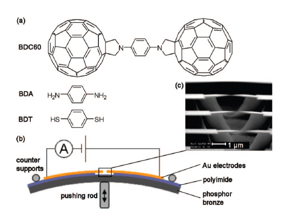
How did the researchers test the effectiveness of these fullerenes as molecular anchors? Using an approach called “mechanically controlled break junction,” they created devices in which the molecules of interest self-assembled in the gap between two gold electrodes.
They then measured the electrical characteristics of these junctions at the molecular level. The results were truly fascinating. Compared to other functional groups commonly used for binding molecules to gold electrodes, such as thiolates and amines, fullerenes showed greater stability and significantly reduced fluctuations in the electronic properties of molecular junctions.
This suggests that fullerenes could play a crucial role in creating more reliable and predictable molecular-scale electronic circuits.
A More Efficient and Sustainable Future
Advances in the use of fullerenes and oligomers in organic photovoltaics and molecular electronics are driving technology towards a more efficient and sustainable future. From improving energy conversion efficiency to developing electronic devices that disintegrate in a controlled manner, these materials promise to revolutionize multiple fields of science and technology.
References:
ACS Appl. Mater. Interfaces 2019, 11, 28138−28144
ACS Appl. Mater. Interfaces 2019, 11, 31069−31077
ACS Appl. Mater. Interfaces 2022, 14, 15461−15467
- Am. Chem. Soc. 2019, 141, 19644−19654
- Am. Chem. Soc. 2020, 142, 11497−11505
- Am. Chem. Soc. 2008, 130, 13198–13199
ACS Appl. Mater. Interfaces 2020, 12, 55064−55071
ACS Appl. Mater. Interfaces 2021, 13, 904−911
Joule 2024, 8, 970–978,
- Am. Chem. Soc. 2008, 130, 13198–13199
RELATED POSTS
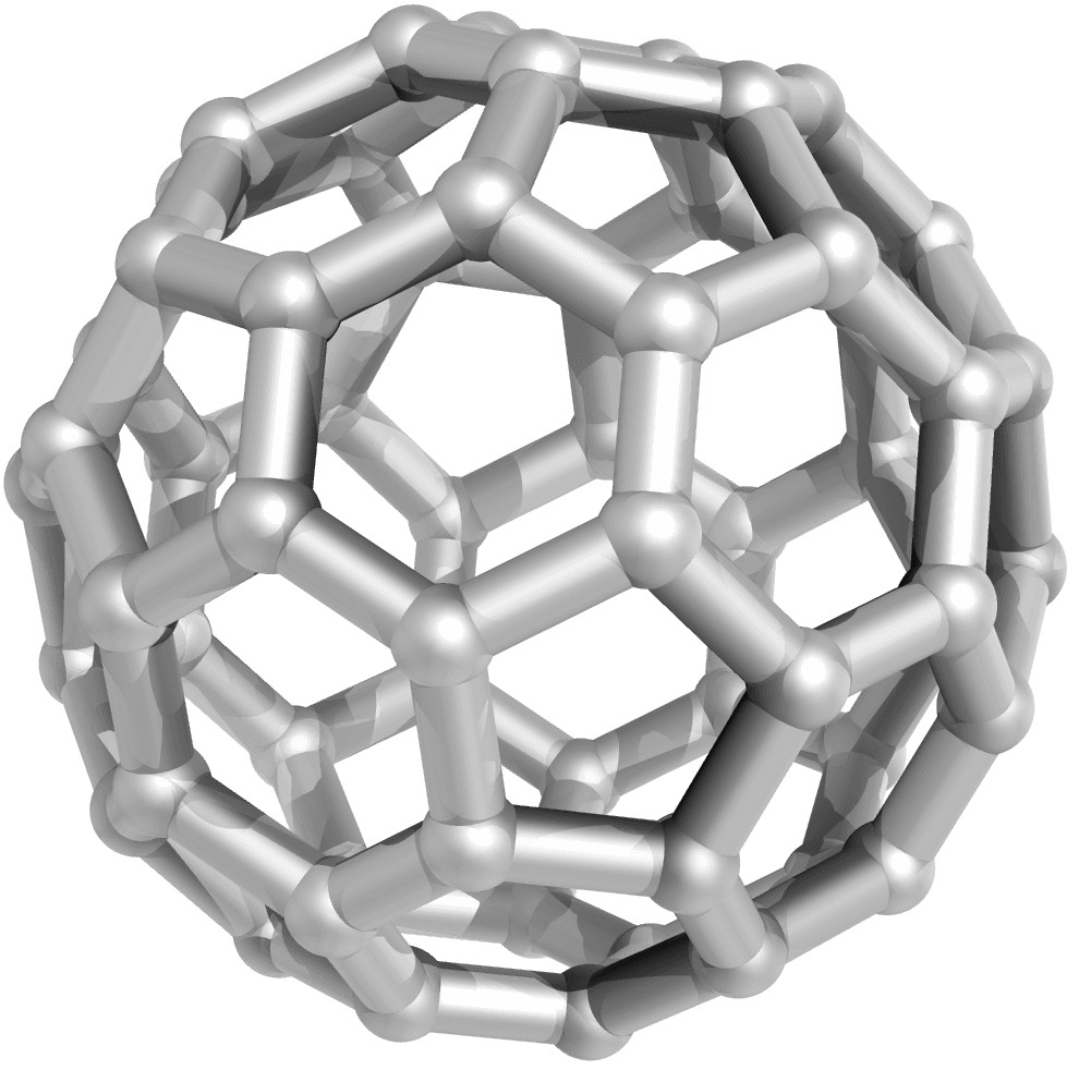
Fullerene C60
Fullerene C60: its unique structures, applications in nanotechnology, electronics, medicine, and advances in organic chemistry and nanomedicine.


